IGBT Printed Circuit Board Reverse Engineering
IGBT Printed Circuit Board Reverse Engineering
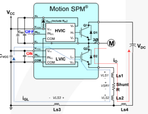
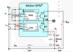
High switching noise may cause a failure in an inverter system. Whenever the IGBT printed circuit board turns on and off, surge voltage is induced due to stray inductance of main current paths on the board. Below Figure include Ls1 and Ls2, which is stray inductance in IGBT Printed Circuit Board Reverse Engineering. High di/dt occurs at transient periods of the IGBT’s turning on and off. This di/dt is induced by the voltage VLS1 and VLS2. It is important to make the traces as short as possible to minimize parasitic inductance.
Above Figure shows low-side gate current (iGL) path through the gate to the emitter of IGBT Q2 and LVIC and VCC to LO when the low-side input signal is on. The low-side IGBT gate charging path includes parasitic inductances and a shunt resistor because LVIC VSL is not connected to the emitter of Q2. Above figure is regarding bootstrap current path (iBS) through the collector to the emitter of IGBT Q2 and VCC, and VB to VS when Q2 or D2 is on. This bootstrap capacitor (CBS) charging current path also includes parasitic inductances and the shunt resistor.


