Reverse Engineering Inverter System PCB
Reverse Engineering Inverter System PCB
Inverter system PCBs are becoming more compact and complex while requiring greater power density. This challenge can be met by adopting a Fairchild Smart Power Module. Reverse Engineering Inverter System PCB layout design is very crucial in improving reliability, performance, and manufacturability while minimizing noise. This application note describes several considerations and guidelines for PCB layout design.
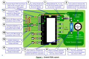
Below Figure shows the overall guidance for PCB layout design, labeled from number 1 to 12 in order of importance.
CONSIDERATION:
Parasitic Inductance, Resistance, and Capacitance
Voltage Spikes from di/dt through the Parasitic Inductance
Route of Power Ground, Signal Ground Layout
Placement of Passive Components


