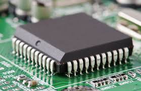
Crack ATmega168A Microprocessor Memory
Crack ATmega168A Microprocessor Memory
The vector is normally a jump to the interrupt routine, and this jump takes three clock cycles. If an interrupt occurs during execution of a multi-cycle instruction, this instruction is completed before the interrupt is served by Crack ATmega168A Microprocessor Memory. If an interrupt occurs when the MCU is in sleep mode, the interrupt execution response time is increased by four clock cycles. This increase comes in addition to the start-up time from the selected sleep mode.
A return from an interrupt handling routine takes four clock cycles. During these four clock cycles, the Program Counter (two bytes) is popped back from the Stack, the Stack Pointer is incremented by two, and the I-bit in SREG is set.
This section describes the different memories in the ATmega168A. The AVR architecture has two main memory spaces, the Data Memory and the Program Memory space. In addition, the ATmega168A features an EEPROM Memory for data storage. All three memory spaces are linear.
The ATmega168 contains 4/8/16K bytes On-chip In-System Reprogrammable Flash memory for program storage. Since all AVR instructions are 16 or 32 bits wide, the Flash is organized as 2/4/8K x 16. For software security, the Flash Program memory space is divided into two sections, Boot Loader Section and Application Program from MCU CRACK.
ATmega168 does not have separate Boot Loader and Application Program sections, and the SPM instruction can be executed from the entire Flash. See SELFPRGEN description in section SPMCSR – Store Program Memory Control and Status Register.
The Flash memory has an endurance of at least 10,000 write/erase cycles. The ATmega48/88/168 Program Counter (PC) is 11/12/13 bits wide, thus addressing the 2/4/8K program memory locations. The operation of Boot Program section and associated Boot Lock bits for software protection are described in detail in ”Self-Programming the Flash, ATmega168.


