PCB Card Track Mutual Inductance
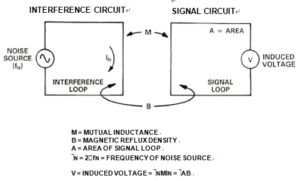
The basic principle is illustrated in below Figure, and is a common mechanism for the transfer of unwanted signals (noise) between two circuits which will generate from PCB Card Track Mutual Inductance.
As with most other noise sources, as soon as we define the working principle, we can see ways of reducing the effect. In this case, reducing any or all of the terms in the equations in above Figure reduces the coupling. Reducing the frequency or amplitude of the current causing the interference may be impracticable, but it is frequently possible to reduce the mutual inductance between the interfering and interfered with circuits by reducing loop areas on one or both sides and, possibly, increasing the distance between them.
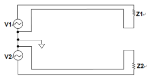
A layout solution is illustrated by below Figure. Here two circuits, shown as Z1 and Z2, are minimized for coupling by keeping each of the loop areas as small as is practical.
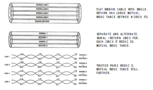
As also illustrated in below Figure, mutual inductance can be a problem in signals transmitted on cables. Mutual inductance is high in ribbon cables, especially when a single return is common to several signal circuits (top). Separate, dedicated signal and return lines for each signal circuit reduces the problem (middle). Using a cable with
Shielding of magnetic fields to reduce mutual inductance is sometimes possible, but is by no means as easy as shielding an electric field with a Faraday shield (following section). HF magnetic fields are blocked by conductive material provided the skin depth in the conductor at the frequency to be screened is much less than the thickness of the conductor, and the screen has no holes (Faraday shields can tolerate small holes, magnetic screens cannot).
LF and DC fields may be screened by a shield made of mumetal sheet. Mu-metal is an alloy having very high permeability, but it is expensive, its magnetic properties are damaged by mechanical stress, and it will saturate if exposed to too high fields. Its use, therefore, should be avoided where possible.


