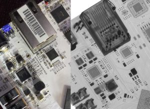
Printed Wiring Board Reverse Engineering Pre-preparation Process
Printed Wiring Board reverse engineering process is undergoing a development process, accompany with the decreasing size of PCB Board dimension and increasing component density, PCB reverse engineering complexity level is raising up. How to realize the high layout yield rate and shorten the reverse engineering time cycle become a hot subject of Printed Wiring Board reverse engineering.
Before we get start to reverse engineering a PCB Board, analysis must be done as well as the installation of reverse engineering software which can help to make the layout drawing, gerber file, schematic diagram and BOM more reasonable and reliable.
First step is decide the printed circuit board layer count:
Printed Wiring Board Dimension and layer count must be decided before the reverse engineering and layout. Since the layer count and the stack-up method will contribute directly to the Printed Circuit Board reverse engineering, layout and impedance. Printed Wiring Board dimension can serve to determine the PRINTED WIRING BOARD stack-UP method and track width and space to achieve the reverse engineering expectation. Currently the cost difference among different number of multilayer Printed Wiring Board is quite small. So it is better to choose the multilayer Printed Wiring Board and ensure the copper spreading is even.
Tags: pcb assemble duplicate,pcb board duplicate,pcb card duplicate,pcb duplicate,pcba duplicate,printed circuit board duplicate,printed wiring board duplicate,pwb duplicate,pwba duplicate


