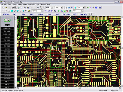
Reverse Engineering PCB Board Layout Diagram Guidelines
Reverse Engineering PCB Board Layout Diagram Guidelines is critical for printed circuit board cloning since it will ensure the correctiveness of the Gerber file;

As long as you follow the following guidelines, good 12-bit wiring skills are not difficult to master:
- Check the position of the components relative to the connector to ensure that the high-speed components and digital components are closest to the connector. There must be at least one ground plane in the circuit wiring diagram reverse design.
- Make the power circuit wider than other traces on the PCB board.
- Check the current loop design from reverse engineering and look for possible noise sources in the ground wire. This can be achieved by determining the current density at all points on the ground plane and the amount of noise that may be present.
- Bypass all devices correctly, and place the capacitor as close as possible to the power supply pin of the device.
- Keep all traces as short as possible.
- Look at all high-impedance traces and look for possible capacitive coupling problems one by one.
- Make sure to properly filter the signal in the mixed signal circuit.

