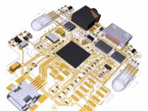
Reverse Engineering Electronic PCB Card Layout Structure
A well performed and precise Electronic PCB Card, except the selected high quality components, reasonable layout, component layout on it, electrical connection and their direction/orientation is also the key of maintaining the reliability of electronic device, as for the circuitry with same component and parameter, the result will have great difference exist due to the variation of component layout design and electrical connection; as a result of that, it is necessary to Reverse Engineering Electronic PCB Card Layout Structure, the correct layout orientation as well as the whole device structure into account, a rational technical structure, can eliminate the noise interference of inappropriate Electronic PCB Card Layout, at the same time, it can facilitate the installation, debugging and maintenance, etc;

Reverse Engineering Electronic PCB Card Layout Structure
Since there is no strictly definition and mode on the excellent structure of Electronic PCB Card Layout, the conclusion extended from below discussion will only be taken as reference. Each one of the circuit board must take corresponding structure design solution according to the electrical functions, structure installation and dashboard layout, and make comparison and repeatable modification among the optional available Electronic PCB Card Layout Structure.
The power supply, and ground databus struction selection which is also name as systematic structure: analog circuitry and digital circuitry must have great amount of difference and equities on the design and layout which can be found when Reverse Engineering Electronic PCB Card Layout Structure. In the analog circuit, due to the existence of amplifier, the minimal noise voltage generated can cause severe distortion on the output signals.
Vice versa, in the digital circuitry, TTL noise limitation is from 0.4V to 0.6V, CMOS noise limitation is only 0.3 to 0.45 times of Vcc, as a result of that, digital circuitry has a better anti-interruption capability; a rational selection from reliable power supply and ground databus is an important guarantee of reliability of our work, tremendous interruption sources will be generated from the power supply and ground databus, among them the noise caused by ground line is the biggest one;

