Placing Component after Reverse Engineering PCB Board
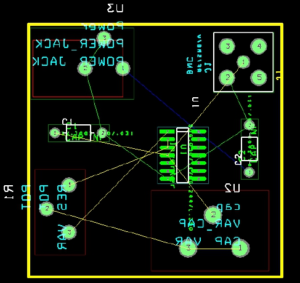
Once the PCB board outline has been specified, it is time to place the components on the PCB board, click on the component icon, and start clicking on the components and strategically place them on the board.
Placing the board is one of most important parts of the Reverse Engineering PCB Board process. If you place the components to close to other components (for instance decoupling capacitors) there will be problems routing, when it is time to route the board.
If however, the components are to far away from each other, the board will play a role in the way that your circuit operates, and your design will not work optimally. Your component layout should be similar to the way you have laid out your schematic diagram however, it is crucial that the analog and digital parts of your circuit are not mixed together. These two parts should clearly separated to reduce noise in your digital circuits.
Note: When placing the board it may be useful to turn the nets (connections) off by clicking on the following icon.
To rotate a component you can click on the component and press “R”. To place a component on the bottom layer, from the top layer, right click on the component and click “opposite”. After the board is placed, it should look something like below Figure.


