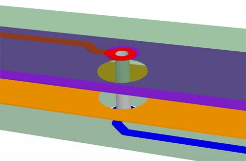
PCB Board Plated Through Hole Development
PCB Board Plated Through Hole Development is the next major advancement that made the PCB board technology indispensable and laid the foundation for what we see today, plated through hole was the ability to put a conductive surface inside a hole in a non-conductive material. This revolution has allowed interconnected circuitry on two sides and through many layers.

PCB Board Plated Through Hole Development is probably the least appreciated major technical advance of the twentieth century, for without it we would not have the ubiquitous electronic products that have become essential to everyday life.
As long as components had leads that penetrated the printed circuit board, the electronic PCB board technology evolved predictably and slowly. However, the introduction of surface mount technology launched another major revolution. With surface mount technology, the component leads did not penetrate the substrate board. PCB technology had to adapt, since the size of components were no longer constrained by the need to provide relatively large through-hole leads.
They could shrink toward the size of the chip itself! It was also possible to use inner-layers without leaving space for holes through the board, which resulted in interconnection structures that were truly three-dimensional. With leads no longer required to go to the perimeter of the component package, they could exit anywhere.
Circuit Board designers and manufacturers were driven to develop the means to access these ever-smaller connection points for further interconnection in the board, usually by penetrating the board with vias, the sole purpose of which was circuit continuity rather than lead connection.

