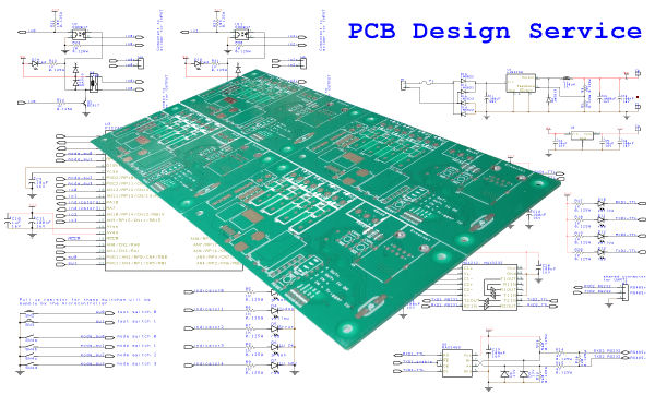
Double Side PCB Board Reverse Engineering
In today’s fiercely competitive battery-powered market, designers often use Double Side PCB Board due to cost constraints. Although the multi-layer PCB board (4-layer, 6-layer and 8-layer) solution has obvious advantages in terms of size, noise and performance, cost pressures have prompted engineers to reconsider their PCB circuit board layout strategy and adopt double-sided PCB board as a the final selection. As a result of that, double side PCB board reverse engineering will become more popular in the market;

In this article, we will discuss the correct and incorrect use of the automatic PCB design layout function, the design strategy of the current loop when there is no ground plane, and the suggestions for the layout of the double-panel components.
The advantages and disadvantages of automatic wiring and the precautions for analog circuit wiring:
When reverse engineering a double side PCB, you often want to use automatic routing. Usually, pure digital circuit boards (especially the signal level is relatively low, the circuit density is relatively small) using automatic wiring is no problem. However, when reverse engineering analog, mixed-signal or high-speed circuit boards, if you use the automatic routing tool of the routing software, some problems may occur, and even serious circuit performance problems may even occur.

